STEM 1
STEM is a project-based learning environment where students learn valuable skills like technical writing, research, collaboration, and project management taught by Dr. Crowthers. The primary focus of this class is an independent research project. Students may choose any topic that interests them to research, the result of which is presented at the Mass Academy Science Fair. The projects presented span many areas including engineering, biology, chemistry, and environmental science.
Identifying the Causation of Voids within Semiconductors to Reduce Waste and Increase Yeild
Project Overveiw
The purpose of this project was to decrease the amount of semiconductors that are unusable due to the formation of voids (small defects) within a semiconductor during manufacturing. I used a form of low-coherence interferometry, called infrared interferometry, where an infrared laser is shot down onto a semiconductor wafer. Based on the light refracted back, a relative depth measurement is returned for that point. Using this method, I measured nearly 150,000 points to map out a semiconductor wafer. I then created a heat map from this data to identify the location of voids throughout the wafer. Based upon this information I was able to make assumptions on where in the semiconductor manufacturing process the identified voids were formed. This data and methodology could be used by semiconductor manufacturers to improve their fabrication process.
Abstracts
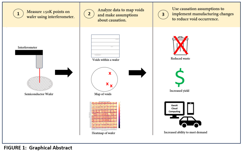 This study explores the use of low-coherence interferometry as a means for identifying voids in semiconductors and their effects based on size, location, and the manufacturing step in which they are introduced. In high-volume semiconductor manufacturing, voids (small defects) can affect the semiconductor in a variety of ways, from intermittent malfunctions to complete failure, resulting in lower yields. Past studies have looked at specific causations, such as a void’s proximity to bond balls, but little has been published about the general features and causation of voids in relation to their impact. Our study will use IR measurements to map voids and the correlation of the voids’ size and locations will be used to identify void causation. Identifying a low-cost method that can be used to identify void causation will enable the semiconductor industry to improve its manufacturing processes and reduce yield loss due to voids. This is important to the industry, as semiconductors power the world’s technologies, from cars to smartphones, and the need for semiconductor chips continues to rise with the increasing demand to support generative AI computing.
Project Proposal
Click here for more info
Problem Statement
Objective
Semiconductors are critical to the world’s technologies, from cars to smartphones, and the need for semiconductor chips continues to rise with the increasing demand to support generative AI computing. Semiconductor manufacturers must ensure the highest yield possible, but today are challenged by voids (small defects) introduced during the manufacturing process. These voids can have various effects on a semiconductor, from intermittent malfunction to complete failure, but it is unknown why different types of voids have varying effects. It is also not clear why voids occur during specific steps in the process. These two gaps in knowledge can make it extremely difficult to develop and implement void mitigation strategies in the semiconductor manufacturing process.
The goal of this project is to identify voids within semiconductors and how steps in the manufacturing process may be causing these voids. Our approach is to utilize Infrared Interferometry (IR), a form of low-coherence interferometry, where a small infrared laser is directed at a silicon wafer. Its reflection is measured and when this measurement changes significantly it represents a void. Once identified, the correlation of the voids’ locations will be used to identify void causation.
Background
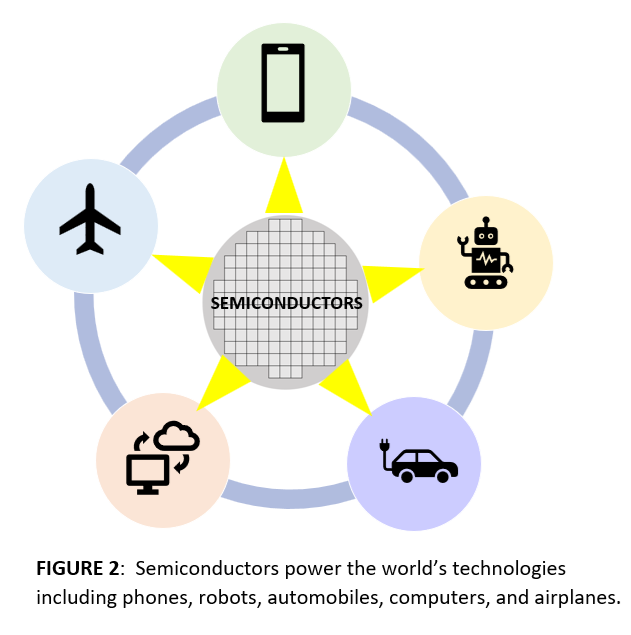 Semiconductors are critical to the world’s technologies, from cars to smartphones, and the need for semiconductor chips continues to rise with the increasing demand to support generative AI computing. This increased demand for semiconductors exemplifies the need to improve product yield and minimize manufacturing defects. Currently, a significant quantity of semiconductors is disposed of within the manufacturing process and pollute the environment. These reduced yields also have an economic effect on the 630-billion-dollar semiconductor industry (Peterson, 2025), as an estimated 1% to 5% of semiconductors produced are defective. This represents an estimated 5.3 to 27.7 billion dollars in lost profit. One of the most common defects that are formed during the manufacturing process are voids. Voids are small pockets of air or moisture that form within a semiconductor during the fabrication. These voids can have various effects on a semiconductor, from intermittent malfunction to complete failure.
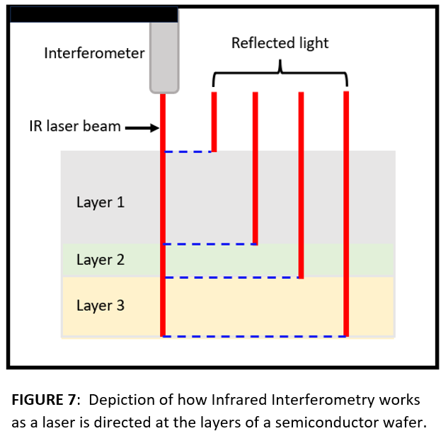
Creating a mitigation strategy for these voids is extremely difficult as they are nanometers in size and invisible to the human eye. Past studies have shown that Infrared Interferometry (IR) is an accurate means for identifying voids, as it is capable of taking measurements with sub-micron accuracy (Poduje, et al., 2010) Infrared Interferometry directs an infrared laser down at a semiconductor wafer and based upon the amount of light reflected, returns a value displaying a relative depth at that point on the wafer. This technology can be used to locate voids by locating depth outliers. These outliers represent voids, as pockets of air and moisture within the wafer affect the light reflected.
Another problem keeping manufacturers from creating mitigation strategies is the lack of knowledge about when voids occur in the manufacturing process. In a 2010 study, researchers were able to find the correlation between how well aligned the layers were and how well bonding adhesive was applied to the number of voids formed. However, this is just a small part of the manufacturing process and does not provide a complete understanding of void formation during the overall fabrication (Rudack, et al.,2010). Developing a way to identify exactly when voids occur throughout the fabrication process will provide the data to make corrections to mitigate their formation.
To help manufacturers increase yield by improving their processes, we must first understand when voids are fatal. Previous studies have been able to correlate the size and location of voids in semiconductors with their performance. In 2004, researchers found that when a void is larger than 100 nanometers in size and is in close proximity to a bond ball (the electrical connection between the silicon and the packaging) it commonly leads to the semiconductor cracking, which is fatal. (Kuo, et al., 2004). Another article calculated a "void distribution uniformity coefficient" to determine consistency. They found that when voids are even, the bonding layer takes the heat flow better and the LED does not get as hot, leading to fewer failures. (Said, et al., 2012.) These studies show that the size and location of a void have a direct relationship with the effect the void has upon the semiconductor.
Some researchers have already begun developing mitigation strategies for voids. One study looked at the benefits of using hybrid bonding and found that it had better electrical connections (that is, fewer voids) resulting in better device performance. They also did a significant amount of testing and found that small voids can lead to failure over time (Jourdon, et al., 2019). This study is a small piece of the puzzle behind a broad problem of void mitigation. It only looks at one strategy and does not compare multiple manufacturing processes or look at individual manufacturing steps. To date, there is little public research published about mitigation strategies for semiconductor production. Most semiconductor companies do not publicly share their manufacturing data.
Procedure
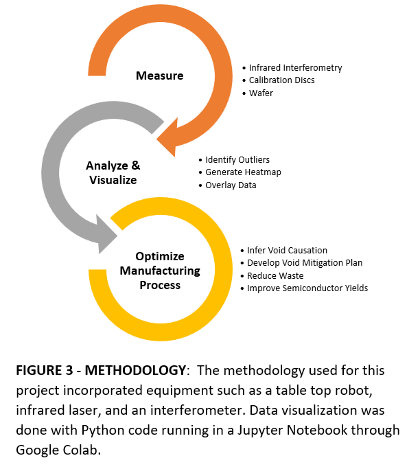 A custom implementation of low-coherence interferometry (LCI) metrology equipment was used to measure the depth at points on a wafer and a calibration disc. The equipment included a tabletop robot (model TT-C2-I-4040 by IAI corporation), an infrared laser, an interferometer, and a PC platform. It worked by having the infrared laser and interferometer connected to the robot arm, which made extremely precise movements to capture measurements at different points. The infrared laser and the interferometer work together by splitting the laser in two. One beam of the laser is reflected straight back at the interferometer. The other beam is directed down at whatever you are trying to measure and based upon the light reflected back towards the interferometer, it calculates the coefficient of light loss. That coefficient can be used as a relative measurement of thickness.
Calibration discs are small discs that have preset measurements that are accurate down to the sub-micron level. They are used to validate the accuracy of measurement techniques.
Silicon wafers are the foundation for manufacturing semiconductors. The wafers I utilized were prepopulated with semiconductor die.
Google Collab is a Jupyter Notebook service that provides free data computing for programmers and data scientists, including the running of Python code. I used the following Python libraries for data analysis and visualization:
• pandas
• seaborn
• matplotlib
• numpy
Technique 1 Infrared Interferometry
Infrared Interferometry is a technique used to find the depth of a target point. Infrared Interferometry works by having an infrared laser and the interferometer work together by splitting the laser in two. One beam of the laser is reflected straight back at the interferometer. The other beam is directed down at what you are trying to measure and based upon the light reflected back towards the interferometer it calculates the coefficient of light loss. That coefficient can be used as a relative measurement of thickness.
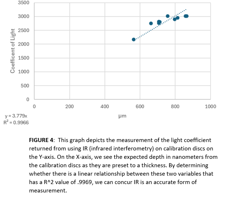
We first attempt to prove the accuracy of this technique by using IR on multiple different calibration discs. Since these discs have a set depth, we can prove IR is accurate down to the sub-micron level as if there is a linear relationship between the actual depth of calibration disc and the value that IR returns then IR is accurate. IR is able to accurately differentiate the depth of these different calibration discs down to the nanometer.
Then, we will use IR to find voids within a semiconductor wafer. We will do this by having IR measure 145,000 points as the tabletop robot moves around the wafer. This will return the depth at all the different points on the wafer. We can use that data to identify where voids are by noting the outliers on the Z coordinate, which then lets us know its X and Y coordinate.
Statistical Tests
To prove the accuracy of IR, I used a R^2 value. I decided on this because an R^2 value shows how well data fits on a line, and I am attempting to prove a linear correlation between the actual depths of calibration discs and the coefficient of light that was returned by IR. This proves that IR is able to accurately measure different depths as for it to have a good R^2 value it must be returning depths in a linear relationship.
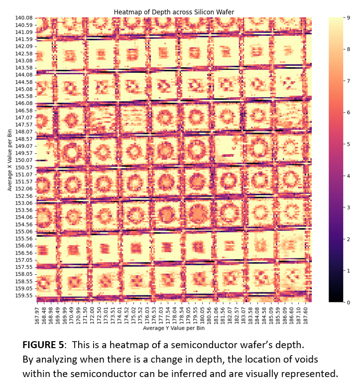
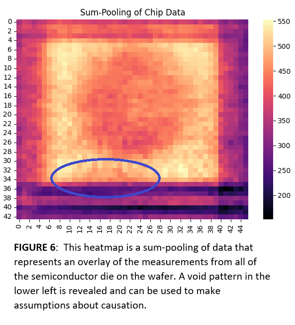
To find the pattern of voids, I made a heatmap of the coefficient of light returned by IR over the X and Y coordinates. With a heatmap of different depths throughout the semiconductor, I then overlaid the data from each die to visualize the average depths of the semiconductor die within the wafer. Patterns that emerge from this test can be used to identify the manufacturing error that caused the defect and help optimize semiconductor production processes.
Analysis
Calibration Disc Test
The results of the first statistical test above display an R^2 value of .9969 meaning that the linear relationship between the calibration disc and the coefficent of light returned is 99.69% fit on the equation Coefficent of Light (Y-axis) equals 3.779 the actual depth in nanometers of the calibration discs (X-axis). The slight variability in the results is most likely due to two factors:
• Human error as I may not have centeed the calibration discs perfectly.
• The calibration discs were older and may no longer be calibrated to their original depth.
This is such a negligable error as it is only a few nanometers . The results prove that IR is an accurate technique at finding depth at the sub-nano level.
Sum-Pooling of Chip Data
The results of the second statistical test are less straight forward. We see within the overlay of all the semiconductor die that voids were forming more frequently within the bottom left of the dies, as seen in the circled part of the image. Due to this pattern, I was able to make the assumption that the error in the manufacturing process of this semiconductor wafer was a bonding error. I made this assumption because pressure and adhesive distribution tend to be less uniform near the edges, making these regions prone to air entrapment creating voids on the edge of the semiconductor die.
Discussion/Conclusion
I was able to prove that IR is an accurate way of locating voids throughout a semiconductor. There was a direct relationship between the known depth of the correlation disc and the coefficient of light that IR returned back to me. This proved that IR was able to accurately measure the depth of different points. Since IR successfully measured the depth, it enabled me to identify outliers, even on the sub-nano scale. These results prove that it is an accurate form of discovering voids.
I was also able to find a pattern in voids of the one semiconductor wafer I tested and make an inference about the error that caused it. However, I was unable to create a true model that would be able to locate where in the manufacturing process an error occurred and what effect it would have based upon statistical evidence. This setback was due to the fact that I was unable to acquire semiconductors or wafers from any of the manufacturers I contacted. Had I secured a partnership with a manufacturer, I would have tested the wafers as they go through each step of the manufacturing process to capture factual evidence regarding when voids are forming. Most semiconductor companies consider their manufacturing processes and defect data proprietary. For this reason, I only had access to a semiconductor wafer used for testing by William Kerr.
Future Research
Next steps for this project would be to partner with a semiconductor manufacturer and receive access to information and wafers that would normally be considered proprietary. I would be able to test their semiconductors at different stages within the manufacturing process and find statistical evidence correlating different voids to different parts of the process. I could also test what effects different voids have upon the semiconductor. Using all this data I could make a model that shows what part of the manufacturing process is causing voids.
Conclusion
During this project I was able to accurately measure, locate, and map voids within a semiconductor using IR. I visualized the IR data with heatmaps to infer which step of the manufacturing process was most likely causing the defect based upon the patterns of voids that emerged in the dies. I also defined a methodology that could be used to create a model that accurately displays when voids were formed and what effect they will have based on their location. I was unable to fully execute this methodology due to not having support from a semiconductor manufacturer. However, future studies could continue this research should a semiconductor company be interested in participating.
Refrences and Poster