STEM One
This course, taught by Dr. Crowthers, is centered around scientific research and engineering principles. In STEM I, students engage in independent research projects, which involve literature review, hypothesis formulation, methodology creation, experimental design, and the dissemination of results. The culmination of their work is showcased at a school-wide science fair, where projects have the potential to progress to regional, state, and global competitions. See below to learn about my project.
Recycling Printed Circuit Boards To Recover Valuable Metals
This year, I have been working on a method to recycle e-waste, specifically printed circuit boards (PCBs), to recover valuable metals. I initially became interested in e-waste several years ago after conducting a project that used machine learning to classify different types of e-waste. My current project is a continuation of this, implementing practices to actually recycle the waste. With the growing importance of metals and e-waste disposal, this process requires far fewer resources and a has smaller ecological footprint compared to existing ones. Implementing these methods in real scenarios has the potential to revolutionize the e-waste recycling industry.
Abstract
In recent years, a growing dependency on technology has led to a significant increase in electronic waste (e-waste), culminating in 53.6 million tonnes in 2019, and heightened demand for metals that are essential for human development, projected to increase 2–6-fold in the next century (Forti et al., 2020; Watari et al., 2021). This situation underscores the urgent need for effective e-waste recycling methods. Traditional recycling techniques are not sustainable, often requiring excessive energy and resources. To solve this problem, this project established a scalable, effective, and sustainable process to obtain valuable metals from printed circuit boards (PCBs), a valuable type of e-waste, through a combination of mechanical and hydrometallurgical methods. The multi-step procedure began with a wet chemical dissolution process using acid to remove electronic components (ECs) from PCBs. Then, mechanical milling and dense medium separation were developed to extract copper from unpopulated PCBs. Finally, the process underwent experimentation, where it was performed under different conditions in hopes of optimization. The results from experimentation suggested that the quickest solution for the EC removal process was 40% vol nitric acid (HNO3), the most effective solution for solder mask removal was potassium hydroxide (KOH), and the optimal solution for dense medium separation was tetrabromethane (TBE) and acetone at a 10:6 ratio. In the future, the recovery of metal from the ECs and reuse of all of the solutions involved in this multistep process will be investigated to improve the yield and environmental friendliness of the entire recycling procedure.
My Research Proposal
Phrase One
The increasing demand for metals and the growing volume of electronic waste in landfills highlight the urgent necessity for the effective recycling of e-waste. Nevertheless, existing recycling techniques are not sustainable and require significant amounts of energy and resources.
Phrase Two
To solve the problem, this project aims to establish a scalable, effective, and sustainable process to reclaim and recycle valuable metals from printed circuit boards through a combination of mechanical and chemical methods.
Background
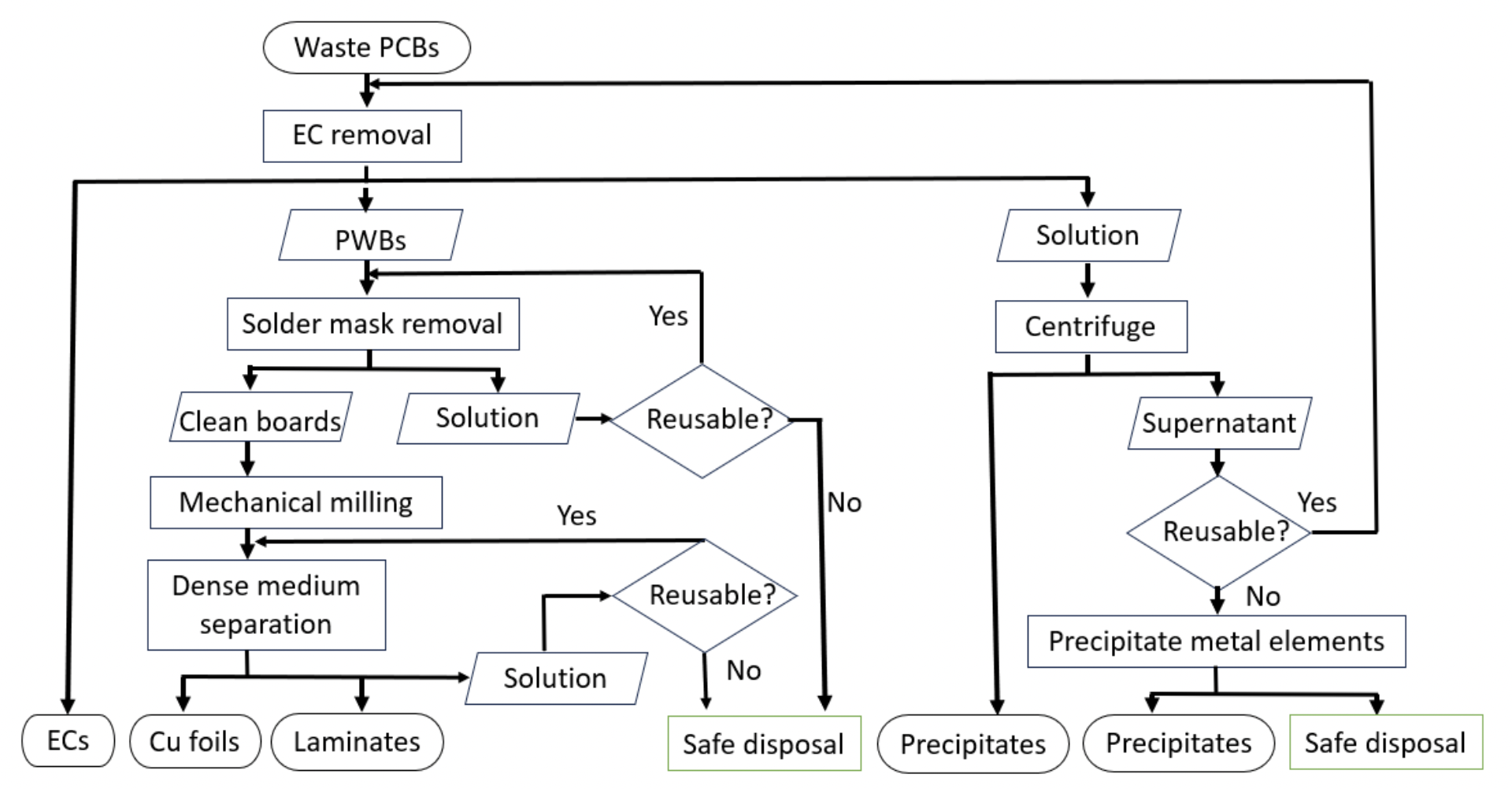
The increasing demand for metals, driven by the rapid expansion of technology and electronics, highlights a critical challenge in resource management and environmental sustainability. At the broader level, this trend reflects a global shift towards greater reliance on technology, impacting not only resource consumption but also waste generation. The global demand for metals is expected to increase approximately 2–6-fold depending on the metal in the 21st century (Watari et al., 2021). In the meantime, the concentrations of useful minerals in ores have been and will invariably continue to decline (Mudd, 2007). These declining ore grades lead to an increase in solid wastes (tailings and waste rock) and energy consumption per unit of metal production. Thus, recovering valuable metals from waste streams becomes critically important to supplying the needed metals for the sustainable development of human society. E-waste is the fastest-growing waste stream in the United States and the world. According to a global study by the United Nations (UN), the world generated 53.6 Mt of e-waste in 2019 (Forti et al., 2020). This amount is projected to grow to 74.7 Mt by 2030. However, the recycling of e-waste is technically challenging due to the complexity of e-waste. Only 17. 4% of e-waste is formally collected and recycled globally (Forti et al., 2020). Printed circuit boards (PCBs) are considered the most valuable e-waste for recycling due to their high content of valuable metals (Golev et al., 2019). In fact, in advanced consumer electronics, PCBs represent more than 80% of the total metal recovery value. Currently, PCBs are either disposed of in landfills or treated by pyrometallurgical methods (Zhu et al., 2023). However, the disposal of PCBs in landfills wastes valuable materials and can release harmful pollutants into the environment through leaching. Pyrometallurgy, or burning PCBs at high temperatures for recovery of valuable metals, is energy-intensive, demands large capital investment, and requires the treatment of harmful gases and dust, such as dioxin or furan (Ahirwar & Tripathi, 2021). The effective recycling of waste PCBs is challenging due to their complexity. As shown in Figure 1, a typical PCB consists of three parts: a plastic laminate substrate, a conducting metal layer on or inside the laminate, which is typically copper, and various electronic components (ECs) such as resistors, chips, and connectors that are mantled on the PCBs by soldering. The laminate substrate with the conducting metal layer is also referred to as a printed wiring board (PWB). To solve the problem, this project established a scalable, effective, and sustainable process to reclaim and recycle valuable metals from PCBs through a combination of mechanical and hydrometallurgical methods. This process consists of multiple steps, including EC dismantling by wet chemical dissolution, solder mask removal by etching, mechanical shredding of the resultant board, and a dense medium separation of the shredded mix. This process requires low capital investment compared with pyrometallurgical methods and is economically and environmentally beneficial compared with pyrometallurgical methods and landfilling. The expected products of this process include ECs, precipitates such as Cu(OH)2 and H2SnO3, and Cu foils. Each product is a valuable feeding stock material that can be sold to well-established specialized companies to repurpose or refine. In future work, the possible reuse and recycling of all of the solutions involved in this multistep process will be investigated further to improve the environmental friendliness of the entire recycling process.
Procedure
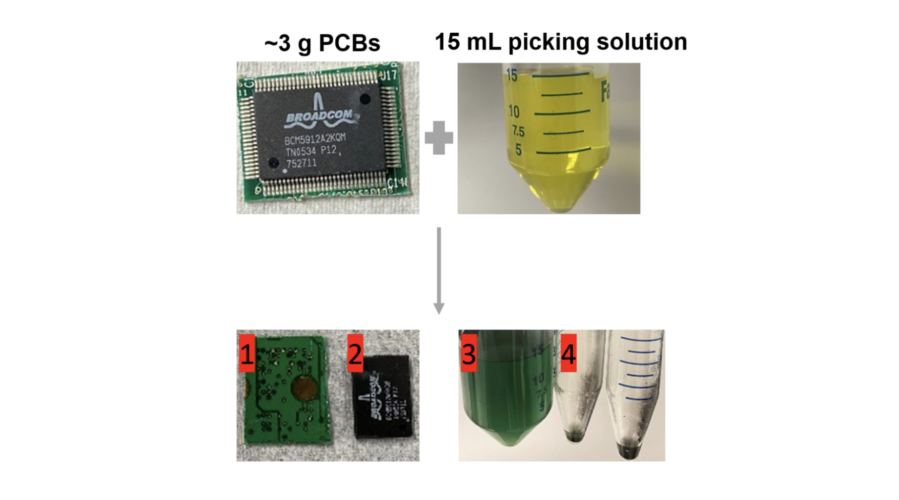
The initial step in recycling printed circuit boards (PCBs) involves removing electronic components (ECs) to retrieve the printed wiring boards (PWBs). This process explored two room temperature methods for disassembling ECs from PCBs. The first method utilized a pickling solution inspired by Tang et al. (2021), consisting of nitric acid, ferric nitrate, ferric chloride, sodium chloride, benzotriazole, and sulfamic acid, with variations in nitric acid concentration while maintaining constant additive levels and a solid-to-liquid ratio of 1g:3ml. This approach facilitates the dissolution of metals like Sn, Pb, and Cu through specific chemical reactions. An alternative method involved a mixture of fluoroboric acid and hydrogen peroxide, as mentioned by Zhang et al. (2015), without a predefined solid-to-liquid ratio, leading to experiments with ratios ranging from 1g:2ml to 1g:9ml over 60 minutes. This solution's effectiveness is attributed to a series of reactions that dissolve metals, highlighting the interaction between hydrogen peroxide, fluoroboric acid, and the metals. Prior to mechanical shredding, solder masks on PWBs were removed using either sodium hydroxide or potassium hydroxide, based on findings by Kang et al. (2021). Experiments with varying concentrations and temperatures sought to optimize conditions for effective solder mask removal. Following this preparation, PWBs underwent mechanical shredding. Subsequently, a dense medium separation technique was applied using a mixture of tetrabromoethane (TBE) and acetone to segregate copper foil from plastic laminate based on density differences, with varied volume ratios to determine the most effective separation conditions. The study also examined the reuse of chemicals in the dismantling process. This included the reapplication of pickling solutions, KOH solutions, and TBE/acetone mixtures, monitoring the effectiveness of each reuse cycle and the stability of the chemicals over multiple rounds. Finally, the residuals from the spent chemical solutions were analyzed using electron dispersive X-ray spectroscopy (EDX) and inductively coupled plasma optical emission spectrometry (ICP-OES) to characterize the precipitates and solutions, providing insights into the chemical alterations and efficacy of the recycling processes.
Figures

Figure 1: Schematic of waste PCB recycling process. Note: 1. Filtration that was used to separate solutions from solids several times in this process is not shown on this schematic flow diagram to make the illustration easy to follow. 2. EC: electronic component. PWB: printed wiring board.

Figure 2: Results of electrical component dismantling by pickling solution. 1. Printed waste board; 2. Electrical component; 3. Used pickling solution; 4. Precipitate obtained by centrifuge.

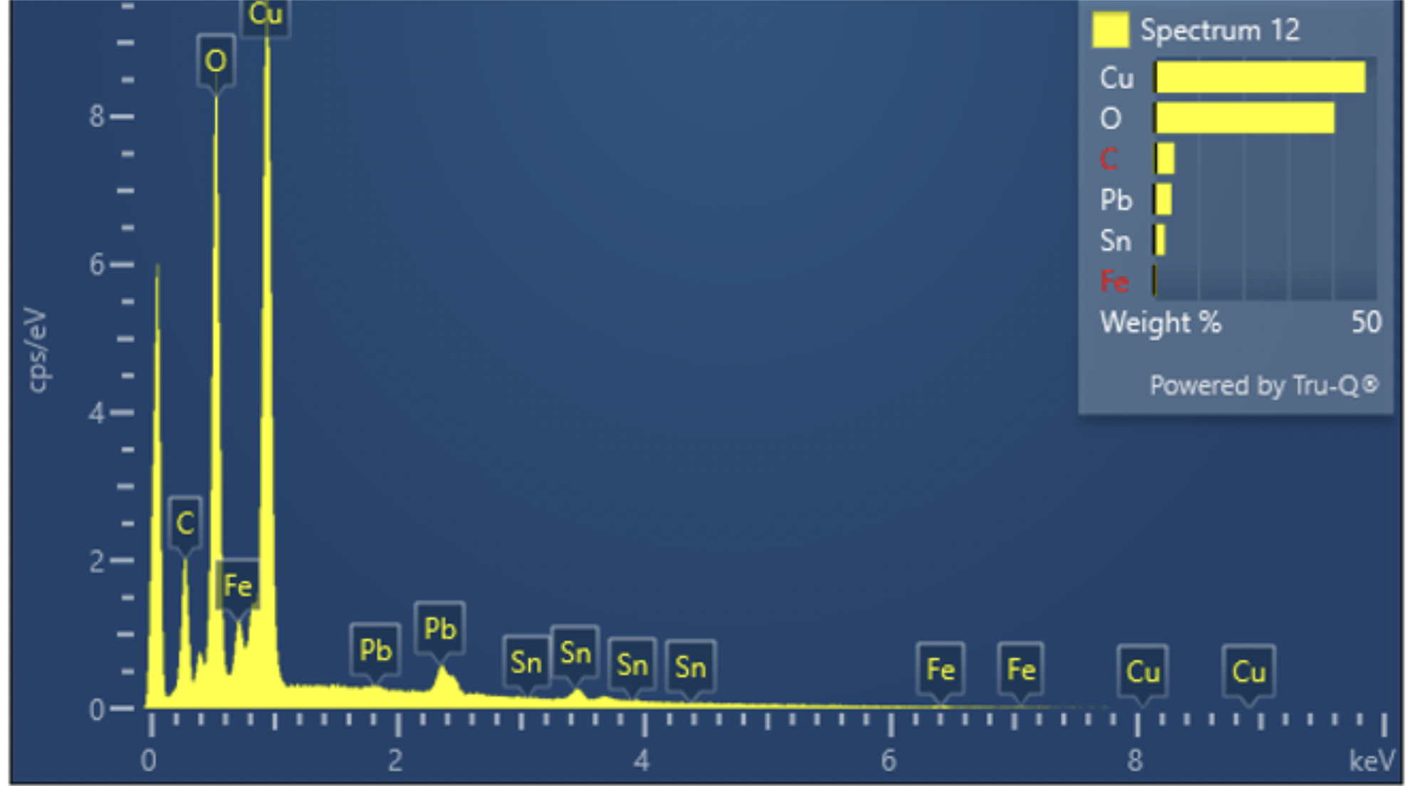
Figure 3: Energy-dispersive X-ray (EDX) analysis result of the precipitates from a potassium hydroxide (KOH) treatment of the used pickling solution.

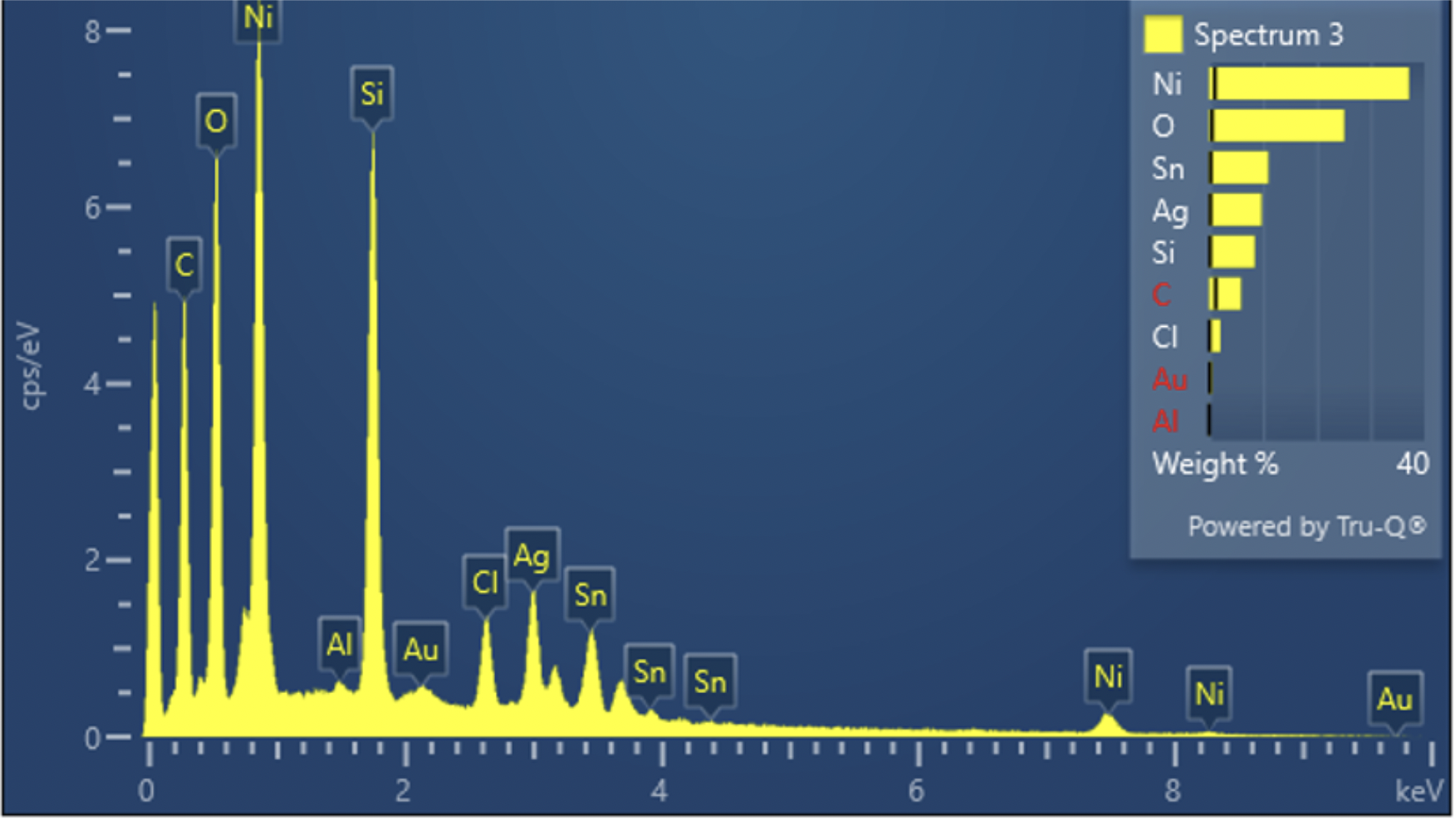
Figure 4: EDX result of the precipitates from the electronic component dismantling by the pickling solution.